
Top 7 PCB layout Tips for Manufacturing
2024-01-19
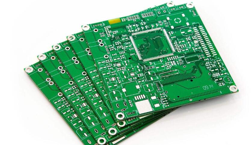
In order to get the best results for your PCB design efforts, you should follow the Design for Manufacturing (DFM) guidelines, which can heavily influence the steps of the PCB manufacturing process and how and if your board can be manufactured. Understanding which manufacturing steps to consider in the design process and successfully addressing them will result in a reliable, high-quality board.
PCB layout is critical for PCB design and manufacturing, but it is crucial. The best way to ensure a well-manufactured and reliable PCB is to work with your contract manufacturer (CM) and follow a simple seven-step PCB layout technique for manufacturing based on the CM's equipment capabilities and processes.
Here are seven of the most important PCB layout tips for the manufacturing process:
Tip 1: Choose the right materials
The first thing to consider in PCB design is to choose the right material. Attributes that may affect the design include thickness, stiffness and flexibility, flame retardancy, color, and the use of high-bandwidth, high-temperature, and high-thermal resistance components. The choice of material affects the manufacturing process, and the specific material selection may vary from CM to CM.
Tip 2: Use the right stacking
The number and type of layers included in the design are important factors that can greatly affect the size of the board, the layout of the drilled holes, the integrity of the signal, the heat dissipation capacity, the electromagnetic capabilities, and the vias. Surface mount equipment (SMD) types, such as ball grid arrays (BGAs) for example, as well as various signal and ground planes, can also affect the arrangement of the layers or the stacking of boards.
Tip 3: Prioritize tracking wiring
Although most designs employ basic traceroute guidelines, there are some important considerations that are sometimes overlooked. When you work with differential signals or high-frequency devices, long, unbalanced, or uneven trace lengths can cause serious problems such as signal distortion, impedance imbalance, and electromagnetic compatibility (EMC) issues. Therefore, it is important to prioritize signal routing. For example, clock and timing devices are routed first, then high-speed and sensitive signals, low-speed signals, and so on. It is also important to separate the analog signal path from the DC as much as possible.
Tip 4: Use the right drill type and size
Almost all PCBs have drilled holes, which may be mounting holes or through-holes. Regardless of your design, you will need to drill the hole according to the drill tolerance and aspect ratio guidelines when positioning, as your options may be limited by CM's drilling equipment.
Tip 5: Confirm that the package is correct
To ensure proper installation of components, it is crucial to ensure that your PCB dimensions match the BOM components. Orientation is correctly placed, including basic markings, such as pin 1 markings for integrated circuits (ICs), and including when and where prohibited foods are recommended by the part manufacturer. Incorrect footprints will most likely require the manufacture of a new board.
Tip 6: Use adequate surface element clearance/spacing
It is also important to space components, traces, and drilled holes according to CM's guidelines. This ensures that the plates can be manufactured and assembled. For example, placing surface components too close together can prevent a solder dam from forming, preventing solder bridges from forming and protecting your board from premature failure due to exposure.
Tip 7: Leave enough board edge space
It is just as important as maintaining adequate spacing between the edges of the plate and proper spacing between surface elements. Designing a PCB layout with insufficient edge clearance can affect the application of solder mask, hindering soldering and board formation, which refers to removing individual boards from panels or sheets used in the manufacturing process.
How to troubleshoot the short circuit fault of PCBA processing
What are the PCB panelization methods?



SEND MESSAGE