

What's PCB Design & Layout Services?
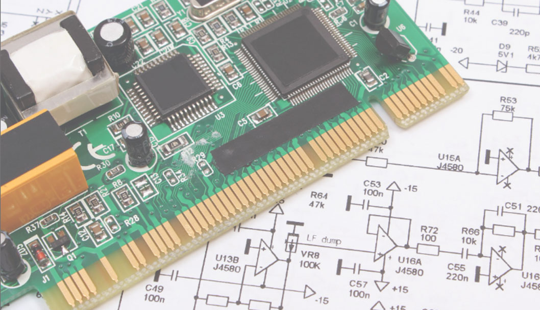
PCB design and layout is the process of converting circuit schematics into physical circuit board layout and connections.
In this process, we need to consider the circuit performance, reliability, EMC (electromagnetic compatibility) and other requirements, but also combine the PCB manufacturing and cost.
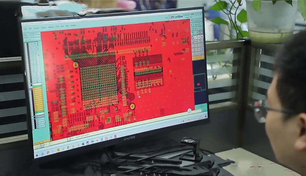
Our PCB Design and Layout Services Including:
-Schematic Design
-PCB Layout Design
-Design for Manufacturability
-Prototype Assembly &Testing
-Design Review & Optimization
-Reverse engineering of PCB
-Design single ended /differential trace layout
-Make customer specific array/panelization
Costomize Design Capabilities
• Hybrid technology, surface mounting, through hole design
• Analog and mixed signal design
• Cavity board design
• Blind via/Buried via/BGA
• High speed digital design
• Analog and mixed signal design
• High speed digital design
• Signal integrity/design verification
• RF PCB design
• Reverse engineering•Sensitive analog circuits
Design Software Used:
Altium,Designer,Eagle,OrCAD,EasyEDA, etc.
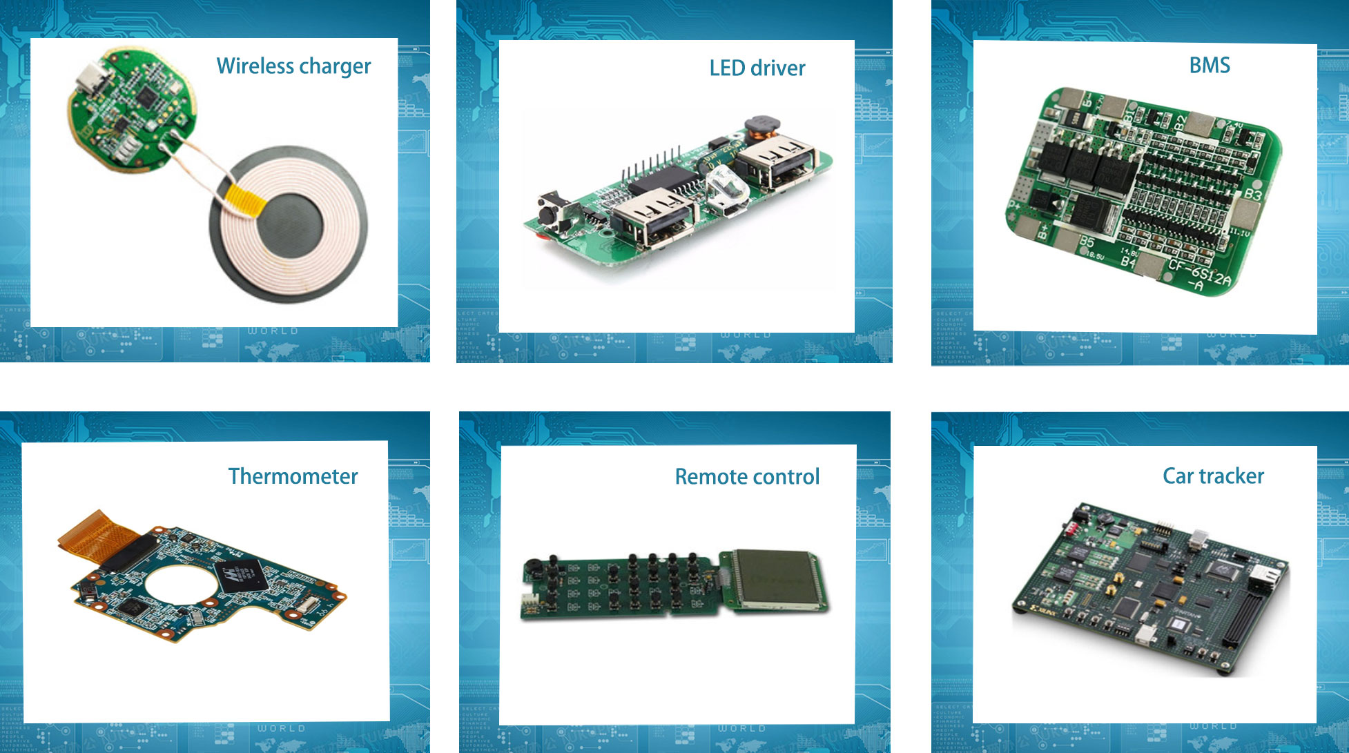
PCB Design Cases For Various Industries
Why Choose Us
SEND MESSAGE