
The importance of PCBA drying and draining
2026-03-05
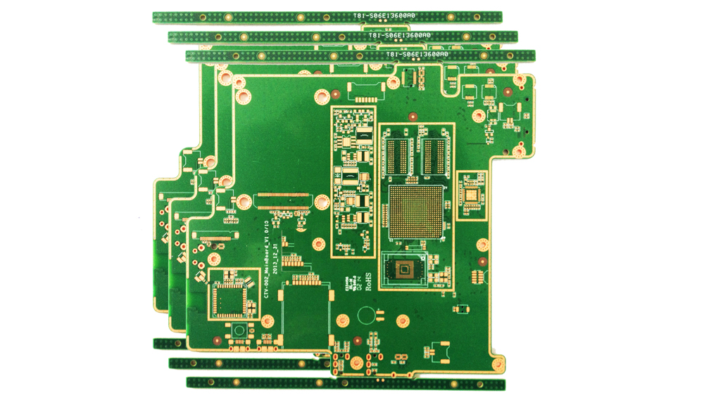
In the processing process of PCBA (Printed Circuit Board Assembly), drying and damp drainage are often overlooked but crucial links. Water vapor is the number one invisible killer of electronic manufacturing, and drying and draining moisture is precisely to eliminate this hidden danger.
1. Prevent the "popcorn effect"
PCB (Printed Circuit Board) substrates are made of epoxy resin and fiberglass cloth, which have some hygroscopic properties. If the circuit board is exposed to humid air before SMT chipping absorbs moisture, when entering the high-temperature area of reflow or wave soldering (usually above 250°C), the moisture inside will instantly vaporize and expand, generating huge steam pressure. This can cause bulging, cracking, or even popping up between chip packages or plates, a phenomenon known as the "popcorn effect." This internal damage is often irreversible and can directly lead to product disconnection or reduced reliability.
2. Eliminate delamination and hole wall fracture
In addition to causing package cracking, excessive moisture can also weaken the bond between the inner layers of the PCB. Under the thermal shock of high-temperature welding, the expansion of water vapor may cause delamination (i.e., peeling between layers) inside the multilayer board, or cause the hole wall to fracture of the through hole wall. These defects are so hidden that they are difficult to detect during routine visual inspections, but they can cause intermittent failures during product use.
3. Avoid solder bead splashing and poor welding
If the PCB or component pins are damp, the water vapor that evaporates rapidly during soldering may splash around with the molten solder, forming fine solder beads on the board. Once these beads fall off, they can cause a short circuit while the device is running. In addition, water vapor can also affect the activity of the flux, leading to poor wetting, false soldering, or soldering defects such as pinholes and blowholes.
The necessity of the post-soldering process in PCBA processing
Common Causes of Solder Mask Defects in PCBA



SEND MESSAGE