
Solutions to common defects in PCB boards
2024-01-29
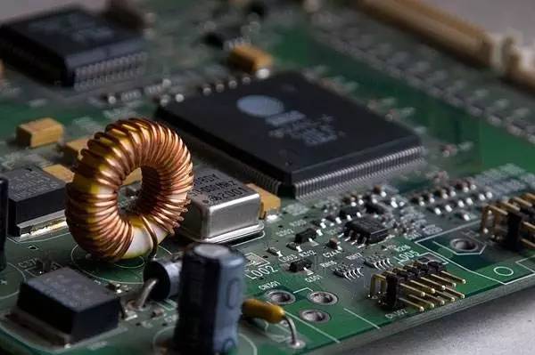
PCB board making is a complex process, in a series of production processes of PCB boarding, there are many matching points, if you are not careful, the board will have defects, and the whole body will be affected, and the quality problems of PCB will emerge in endlessly, such as short circuits, open circuits, etc., and then STG Electronic will introduce the common bad causes of PCB boards.
Common causes of defective PCB boarding
1. Short circuit
(1) The pad design is improper, we can change the round pad to an oval shape, increase the distance between the dots, and prevent short circuit.
(2) The orientation of the PCB part is not properly designed, for example, if the feet of the SOIC are parallel to the tin wave, it will cause a short circuit, so we can modify the part orientation appropriately so that it is perpendicular to the tin wave.
(3) Automatic plug-in bending feet, will also cause PCB short circuit, because the IPC stipulates that the length of the wire pin is less than 2mm, and there is a concern that the part will fall when the bending angle is too large, so it is easy to cause a short circuit, so the solder joint should be more than 2mm away from the line.
In addition to the above 3 points, there are some reasons that will cause the problem of short circuit of the PCB board, such as the substrate hole is too large, the temperature of the tin pot is too low, the solderability of the board surface is poor, the solder mask fails, the board surface is contaminated, etc., engineers can carry out a series of troubleshooting for the above reasons.
2. Open the road
An open circuit occurs when the trace breaks, or when the solder is only on the pad and not on the component lead.
This is because there is no adhesion or connection between the component and the PCB, just like a short circuit, which can occur during production or soldering and other operations.
Vibration or stretching of the boards, dropping them, or other mechanical deformation factors can damage traces or solder joints.
Chemicals or moisture can cause wear and tear on solder or metal parts, which can lead to component leads breakage.
3. Dark and granular contacts appear on the PCB board
Most of the problems that occur on the PCB are due to the contamination of the solder and the excessive amount of oxides mixed in the tin, resulting in a brittle solder joint structure. Care should be taken not to confuse it with the dark color caused by using solder with a low tin content.
Another reason for this problem is that the composition of the solder used in the manufacturing process changes, and the impurity content is too much, so it is necessary to add pure tin or replace the solder.
Speckled glass is caused by physical changes in the fiber lamination, such as the separation of layers from one layer.
However, in this case, it is not that the solder joints are defective, but that the substrate is overheated, so it is enough to reduce the preheating and soldering temperature or increase the speed of the substrate.
4. The solder joints of the PCB board turn golden yellow
Normally, the solder of the PCB board is silver-gray, but occasionally there are golden-yellow solder joints. The main cause of this problem is that the temperature is too high, so you only need to lower the temperature of the tin pot.
5. Environmental impact
In the environment of extreme temperature or temperature fluctuation, excessive humidity, high-intensity vibration, etc., it is easy to cause damage to the PCB board. For example, changes in ambient temperature can cause deformation of the board, which can damage solder joints, bend the shape of the board, or cause copper traces on the PCB to break.
Moisture in the air can cause oxidation, corrosion and rust on metal surfaces, such as exposed copper traces, solder joints, pads and component leads.
Accumulation of dirt, dust, or debris on the surface of components and PCBs can reduce air flow and cooling of parts, resulting in PCB overheating and performance degradation.
Vibration, dropping, hitting or bending a PCB can deform or crack it, while high currents or overvoltages can cause the PCB board to break down or components and paths to deteriorate rapidly.
Advantages and disadvantages of PCB surface treatment process OSP
The role of circuit board grounding and common grounding methods



SEND MESSAGE