
Advantages and disadvantages of PCB surface treatment process OSP
2024-01-30
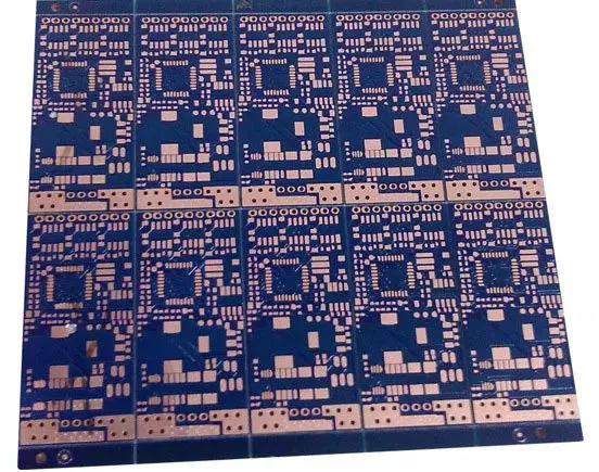
Advantages and disadvantages of OSP, the surface treatment process of PCB board making. OSP is organic solder film, also known as copper protection agent, which mainly plays a certain role in protecting copper exposed to air, which is a common surface treatment process in PCB processing. Everything is not perfect, OSP is no exception, and then STG Electronics will introduce the advantages and disadvantages of OSP in the surface treatment process of PCB boarding.
The role of OSP
OSP acts as a barrier between copper and air, which is what makes it different from other surface treatment processes, as OSP is organic, not metal, so it is cheaper than tin-spraying. The principle is to chemically grow an organic film on a clean bare copper surface, and many computer motherboards use the OSP process.
This layer of organic film can ensure that the inner layer of copper foil will not be oxidized before soldering, and when soldering, once heated, this film will volatilize, and the solder can solder the copper wire and components together.
Advantages and disadvantages of OSP
Merit:
With all the advantages of bare copper plate welding, expired boards can also be resurfaced.
Shortcoming:
1. OSP is transparent and colorless, which is difficult to inspect, and it is difficult to distinguish whether it has been treated by OSP.
2. OSP itself is insulated and non-conductive, which will affect the electrical test. In this way, the test point must be printed with solder paste on the stencil to remove the original OSP layer before it can contact the pin point for electrical testing. OSPs cannot be used to handle electrical contact surfaces, such as keyboard surfaces for keys.
3. OSP is not corrosion-resistant, and is easily affected by acid and temperature. When used for secondary reflow soldering, it needs to be completed within a certain period of time, and usually the effect of second reflow soldering will be relatively poor. If it is stored for more than three months, it must be re-surfaced and used within 24 hours after opening the package.
An OSP circuit board that has been exposed to air for more than ten days cannot solder components.
Why does flux residue on an assembled printed circuit board cause electrical failure?
Solutions to common defects in PCB boards



SEND MESSAGE