
Why do we need to panelize PCB?
2026-02-07
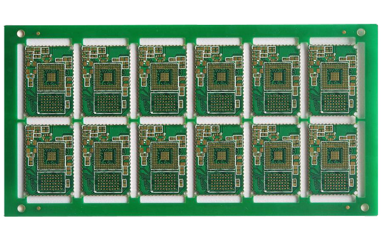
PCB panelization, which involves combining multiple individual PCB units onto a single larger board for production, is a key and cost-effective process in modern electronics manufacturing. Its main purpose is to significantly improve overall efficiency, reduce costs, and ensure the reliability and consistency of the production and assembly process through standardized, large-scale manufacturing. The specific reasons can be summarized in four aspects:
First, to maximize production efficiency and economic benefits. Modern PCB manufacturing and SMT assembly equipment (such as exposure machines, etching lines, and pick-and-place machines) are optimized for standard-sized boards. By combining dozens or even hundreds of small PCB units into a standard-size large board (such as 18" × 24") for production, the number of board loading, alignment, and line change operations can be greatly reduced. Especially in the placement stage, the pick-and-place machine can complete the mounting of all components on the entire board in a single run, increasing efficiency by several dozen times. At the same time, panelization effectively reduces board scrap and improves raw material utilization, significantly lowering the unit cost of a single PCB.
Second, to meet automation production requirements and ensure process quality. Very small, irregularly shaped, or thin individual PCBs are prone to jamming or shifting on automated production lines and cannot be conveyed stably. After panelization, the resulting "production board" has sufficient mechanical strength and a regular shape, ensuring stable operation on SMT production lines, wave soldering machines, and test fixtures. In addition, producing the entire board ensures that all units undergo completely consistent printing, soldering, and cleaning processes, facilitating stable control of process parameters and enhancing product quality consistency. Automated optical inspection (AOI) and electrical performance testing can also scan the entire board at once, greatly improving testing efficiency.
Third, to address specific design challenges and facilitate subsequent processing. For PCBs with irregular shapes or cutouts, panelization can provide regular outer frames and process edges, making it easier for machines to hold and position them. Optical alignment marks (Mark points) and positioning holes can be added on the process edges, which are essential for high-precision placement. At the same time, standard methods such as V-CUTs or mouse-hole stamp connections lay the foundation for efficient and standardized board separation later.
Finally, panelization also supports mixed panelization, allowing different PCB designs to be combined on one large board. This is particularly suitable for prototyping or small-batch production of multiple varieties, greatly shortening delivery cycles and reducing costs.
In summary, PCB panelization is a key bridge between ideal circuit design and industrial production reality. By integrating and optimizing, it transforms scattered manufacturing needs into batch-able, stable, and efficient "industrial semi-finished products." It is a core process for balancing cost, efficiency, and quality, supporting the rapid and reliable manufacturing system of modern electronic products.
Why is surface treatment necessary for PCB board?
How Does the Quality of Conformal Coating Affect PCBA Circuit Boards?



SEND MESSAGE