
PCB assembly inspection and testing options Guide
2023-11-17
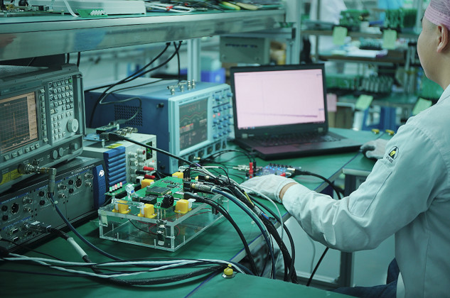
As technology advances and PCBA become increasingly complex, the testing and inspection options for these boards must be carefully considered. PCBS are key components that are expected to function properly in a variety of different environments. Appropriate testing procedures and inspection measures are required to maintain product quality and reliability.
PCB inspection and testing benefits
Having a trusted contract manufacturer is one of the most critical steps to successfully building a board. Vinatronic prides itself on providing high quality products to its customers. This is done through our PCB assembly manufacturing process, which has been iterated over several years. We pay close attention to preventative measures and pre-build steps, rather than finding problems at a later stage and fixing defects through rework.
The most common inspection and testing methods are:
· Vision examination
· Automated optical inspection
· X-ray examination
· First piece inspection
· Online testing
· Functional testing
· Burn-in test
PCB come in a variety of different shapes, sizes and quality requirements. They can be rigid or flexible, single-sided, double-sided, multi-layered, and others. The industry also uses three "categories" to classify PCBS and PCbas. These are levels 1, 2 and 3, with level 3 being the highest quality and requiring the most attention.
As the level requirements increase, so does the complexity of inspection and testing methods. Both PCB manufacturing and PCB assembly require a unique set of inspection and test methods in order to manufacture the board to specifications.
Visual examination
The most basic form of inspection is visual inspection. This is done by having technicians review circuit boards with gold boards, bills of materials, and prints. The person then checks for faulty components, missing components, welding Bridges, missing solder, forgotten tombstones, and various other errors. Equipment that can be used includes magnifying glasses, high-power microscopes, and of course, very good lighting. Because this method is highly operator dependent, it can be time consuming for large and complex boards. This is mainly done at the end, but it is important to visually inspect the board throughout the manufacturing process to verify procedures and procedures. An inspection after SMT placement can reveal missing or incorrect component placement and solder paste problems on the pick and place machine.

Automatic Optical Inspection (AOI)
AOI utilizes high-resolution cameras and software to catch manufacturing errors. The software essentially examines multiple images of the inspected circuit board against the "gold" circuit board image stored in its memory and flags the differences.
These machines can be placed on the entire SMT production line. An inspection after the reflow stage can reveal defects in the welding, such as dry solder, solder bridging, insufficient wetting, tombstone shedding, etc. The operator can then use feedback from the machine to make finer adjustments to previous stages to ensure fewer defects.
Although AOI technology has come a long way, it still has some drawbacks. On the one hand, AOI does not do a good job in through-hole parts. It can catch a lot of through-hole errors, such as wrong parts or missing parts, but sometimes height differences, cast shadows and hidden parts can be limitations of AOI. Programming also takes a while, which is an additional overhead.

X-ray examination
For components with hidden leads, X-ray inspection is required. The underside of the BGA is arranged with pins, which makes it impossible to optically check its connection after welding. X-rays are then used to check that all leads are properly welded.

SMT first article inspection
In order to verify programs and components, the original equipment manufacturer usually requires a first inspection. Companies' FAI programs vary, with some requiring written documentation from the CM verifying the completion of the FAI and others requiring the first article to be actually sent to them for approval. Whatever your company deems necessary, it is important to communicate with CM to check all boxes.

Online and functional testing
Online testing: This form of testing requires custom fixtures, often referred to as nail beds. Usually several spring-loaded metal probes are mounted in an array on an insulated bed. If ICT testing is seen as the best form of testing, it is usually planned during the design phase, as this requires the designer to place the test pad in a key location on the underlying copper wiring of the PCB.

The tester places the assembled PCB on the probe to electrically connect it to the test pad. Sometimes this is handmade or built into a light fixture. The test will then check various parameters, such as the resistance, capacitance, and inductance between the specified probes, as well as the marker differences from the established standards.
Functional testing: This method is highly variable. It essentially simulates equipment in the field. This form of testing is created by the OEM and given to the CM to run. It usually includes a power supply and several inputs to ensure that the board works as expected.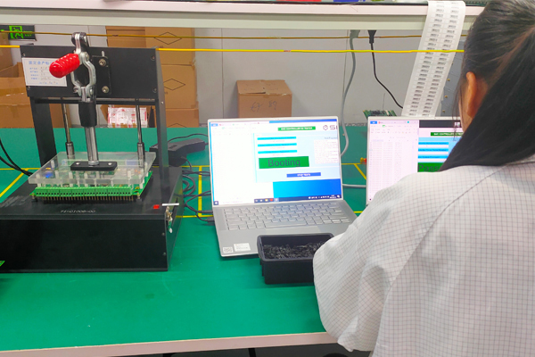
Aging test
Burn-in tests simulate real-world environments. The PCB components will be cooled at high temperatures starting from 24 hours and set for a specified time after cooling, and there should be no expected performance issues. This can be verified by functional testing or ICT.

The importance and analysis of PCB circuit board heat dissipation design
What is Surface Mount BGA package?



SEND MESSAGE