
Explain in detail the basic requirements of PCB prototype multilayer board design
2024-02-28
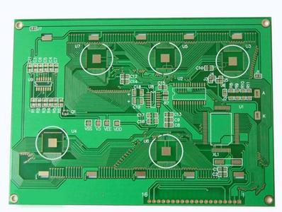
Determination of board shape, size and number of layers
Any printed board has the problem of matching and assembling with other structural parts, so the shape and size of the printed board must be based on the structure of the whole machine. However, from the perspective of production technology, it should be as simple as possible, generally a rectangle with a small difference in aspect ratio, so as to facilitate assembly, improve production efficiency and reduce labor costs.
In terms of the number of layers, it must be determined according to the requirements of circuit performance, board size and line density. For PCB multilayer boards, four-layer boards and six-layer boards are the most widely used, taking four-layer boards as an example, there are two wire layers (component surface and soldering surface), a power layer and a ground layer.
The layers of the multi-layer board should be symmetrical, and preferably an even number of copper layers, i.e., four, six, eight layers, etc. Because of the asymmetrical lamination, the board surface is prone to warping, especially for surface-mounted multilayer boards, which should be paid more attention.
The position and orientation of the components
The position and direction of the components should first be considered from the aspect of the circuit principle to cater to the direction of the circuit. The reasonable placement will directly affect the performance of the printed board, especially the high-frequency analog circuit, and the requirements for the position and placement of the device are more stringent. Proper placement of components, in a sense, already bodes well for the success of this PCB design. Therefore, when starting to arrange the layout of the printed board and determine the overall layout, we should conduct a detailed analysis of the circuit principle, first determine the location of special components (such as large-scale ICs, high-power tubes, signal sources, etc.), and then arrange other components to avoid factors that may cause interference.
On the other hand, the overall structure of the printed board should be considered to avoid uneven and chaotic arrangement of components. This not only affects the aesthetics of the printed board, but also brings a lot of inconvenience to the assembly and maintenance work.
Requirements for wire layout and wiring area
In general, the PCB multi-layer board wiring is carried out according to the circuit function, and when the outer layer is wiring, it is required to wiring more on the soldering surface and less wiring on the component surface, which is conducive to the maintenance and troubleshooting of the printed board. Thin, dense wires and signal lines that are susceptible to interference are usually arranged in the inner layer. A large area of copper foil should be evenly distributed in the inner and outer layers, which will help to reduce the warpage of the board and also make the surface more uniform plating during plating. In order to prevent the short circuit between the layers caused by the printed wire and the machining process, the distance between the conductive pattern of the inner and outer wiring area and the board edge should be greater than 50mil.
Requirements for conductor direction and line width
The PCB multi-layer board wiring should separate the power layer, ground layer and signal layer to reduce the interference between power supply, ground and signal. The lines of the two adjacent layers of printed boards should be perpendicular to each other or diagonal lines and curves as far as possible, and should not be parallel, so as to reduce the interlayer coupling and interference of the substrate. And the wire should be as short as possible, especially for small signal circuits, the shorter the wire, the smaller the resistance, the smaller the interference. The signal line on the same layer should avoid sharp corners when changing direction. The width of the wire should be determined according to the requirements of the circuit for current and impedance, the power input line should be larger, and the signal line should be relatively smaller. For general digital boards, the power input line width can be 50~80mil, and the signal line width can be 6~10mil. The relationship between the current and resistance of the printed board wire and the allowable passage is as follows:
Wire width (mm)
Allowable Current(A)
Wire resistance (Ω/m)
0.5
0.8
0.7
1
1
0.41
1.5
1.5
0.31
2
1.9
0.25
When PCB proofing and wiring, it should also be noted that the width of the line should be as consistent as possible to avoid the sudden thickening and thinning of the wire, which is conducive to the matching of impedance.
Drill hole size and pad requirements
The drilling size of the components on the PCB multilayer board is related to the pin size of the selected components, the drilling hole is too small, which will affect the assembly and tin of the device, and the drilling hole is too large, and the solder joint is not full enough during soldering. In general, the component hole diameter and pad size are calculated as follows:
Aperture of component hole = component pin diameter (or diagonal) + (10~30mil)
Component pad diameter ≥ component hole diameter +18mil
As for the pore diameter, it is mainly determined by the thickness of the finished board, and for high-density multilayer boards, it should generally be controlled in the range of plate thickness: pore diameter ≤5:1. The calculation method for via pads is:
VIA PAD diameter ≥ via diameter +12mil.
Requirements for power layer, formation partition and perforation:
For PCB multilayer boards, there is at least one power layer and one ground layer. Because all the voltages on the printed board are connected to the same power supply layer, the power layer must be partitioned and isolated, and the size of the partition line is generally 20~80mil line width.
In order to increase its reliability and reduce the virtual welding caused by heat absorption in a large area of metal during the welding process, the general connection plate should be designed in the shape of a perforation
The hole diameter of the isolated pad ≥ the drilling hole diameter +20mil
Safety distancing requirements
The setting of PCB proofing safety spacing should meet the requirements of electrical safety. Generally speaking, the minimum spacing of the outer conductor shall not be less than 4mil, and the minimum spacing of the inner conductor shall not be less than 4mil. In the case that the wiring can be arranged, the spacing should be as large as possible to improve the yield rate of the board and reduce the hidden danger of the failure of the finished board.
The requirements for improving the anti-interference ability of the whole board
In the design of PCB multilayer boards, we must also pay attention to the anti-interference ability of the whole board, and the general methods are:
a. Add filter capacitors near the power supply and ground of each IC, and the capacitance is generally 473 or 104.
b. For sensitive signals on the printed board, accompanying shielded wires should be added separately, and as little wiring as possible near the signal source.
c. Choose a reasonable grounding point.
How to solve the problem that the PCB board has solder balls?
Why are most of the circuit board PCB green?



SEND MESSAGE