
Common Defects in PCB Pad During Wave Soldering and Their Solutions
2025-06-25
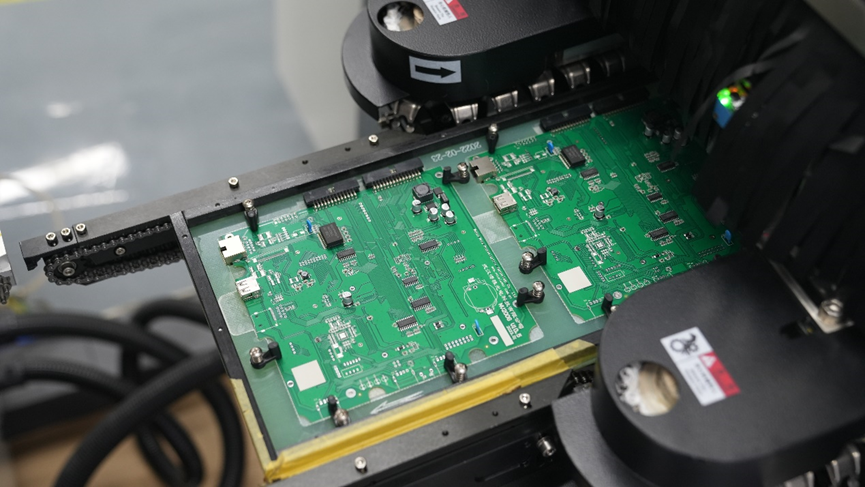
PCB Pad Defects in Wave Soldering: Causes & Remedies
1. Introduction
Wave soldering is widely used for through-hole (THT) and mixed-technology PCB assembly. However, improper process control can lead to pad-related defects, affecting reliability. Below are common issues, root causes, and corrective actions.
2. Common Defects & Solutions
2.1 Solder Bridging
- Description: Unintended solder connections between adjacent pads or pins.
- Causes:
- Excessive solder wave height or contact time.
- Incorrect pad spacing (DFM violation).
- Poor flux activity or contamination.
- Incorrect pad spacing (DFM violation).
- Poor flux activity or contamination.
- Solutions:
- Optimize wave height and conveyor speed.
- Redesign PCB with adequate pad-to-pad clearance (≥0.5mm).
- Use solder masks or "thieving pads" to reduce solder accumulation.
- Redesign PCB with adequate pad-to-pad clearance (≥0.5mm).
- Use solder masks or "thieving pads" to reduce solder accumulation.
2.2 Poor Wetting (Non-Wetting/De-Wetting)
- Description: Solder fails to adhere to pads, leaving exposed copper or uneven coverage.
- Causes:
- Oxidation on pads or component leads.
- Insufficient flux application or inactive flux.
- Low solder temperature or contaminated solder bath.
- Insufficient flux application or inactive flux.
- Low solder temperature or contaminated solder bath.
- Solutions:
- Pre-clean PCBs (e.g., plasma cleaning) and store in moisture-free environments.
- Increase flux spray volume or switch to no-clean flux.
- Monitor solder pot temperature (typically 250–265°C for Sn-Pb, 260–280°C for lead-free).
- Increase flux spray volume or switch to no-clean flux.
- Monitor solder pot temperature (typically 250–265°C for Sn-Pb, 260–280°C for lead-free).
2.3 Pad Lifting (Delamination)
- Description: Pads separate from the PCB substrate due to mechanical/thermal stress.
- Causes:
- Excessive thermal shock during soldering.
- Weak pad adhesion (poor PCB fabrication).
- Mechanical stress during lead trimming.
- Weak pad adhesion (poor PCB fabrication).
- Mechanical stress during lead trimming.
- Solutions:
- Reduce wave contact time and preheat temperature (gradual thermal profiling).
- Specify high-Tg (glass transition temperature) laminates for multilayer PCBs.
- Avoid manual lead bending after soldering.
- Specify high-Tg (glass transition temperature) laminates for multilayer PCBs.
- Avoid manual lead bending after soldering.
2.4 Solder Balling
- Description: Small solder spheres trapped near pads or under components.
- Causes:
- Moisture absorption in PCBs or components.
- Solder splash due to violent wave turbulence.
- Incompatible flux volatility.
- Solder splash due to violent wave turbulence.
- Incompatible flux volatility.
- Solutions:
- Bake moisture-sensitive PCBs (e.g., 125°C for 4–8 hours) before soldering.
- Adjust wave nozzle geometry to reduce turbulence.
- Use low-spatter flux formulations.
- Adjust wave nozzle geometry to reduce turbulence.
- Use low-spatter flux formulations.
2.5 Voiding (in Plated Through-Holes, PTHs)
- Description: Air pockets trapped in solder joints, reducing mechanical strength.
- Causes:
- Gas escape from contaminated/vias during soldering.
- Insufficient hole-fill due to low solder temperature or poor flux penetration.
- Insufficient hole-fill due to low solder temperature or poor flux penetration.
- Solutions:
- Ensure proper PTH copper plating quality (IPC Class 2/3 standards).
- Increase preheat temperature (90–120°C) to volatilize contaminants.
- Use vacuum-assisted wave soldering for critical applications.
- Increase preheat temperature (90–120°C) to volatilize contaminants.
- Use vacuum-assisted wave soldering for critical applications.
3. Process Optimization Tips
1. Preheat Stage:
- Maintain 90–120°C to activate flux and prevent thermal shock.
2. Flux Application:
- Select spray/foam flux compatible with solder alloy (e.g., ROSIN-based for Sn-Pb).
3. Wave Parameters:
- Chip wave: For SMD retention; lambda wave: For THT filling.
- Contact time: 3–5 seconds.
4. Post-Soldering:
- Inspect with AOI/X-ray and clean residues (if non-no-clean flux is used).
4. Key Standards for Quality Control
- IPC-A-610: Acceptance criteria for solder joints.
- IPC-J-STD-003: Solderability requirements for PCBs.
- IPC-7351: Pad design guidelines to prevent defects.
5. Conclusion
Defects in wave soldering often stem from design, material, or process issues. Implementing DFM checks, strict process controls, and post-solder inspections can significantly reduce failures.
Methods for Waterproofing, Moisture-proofing, and Corrosion Resistance in PCBA Circuit Boards
Temperature Resistance of PCB Boards in SMT Assembly



SEND MESSAGE