
Common Causes of Solder Mask Defects in PCBA
2026-03-04
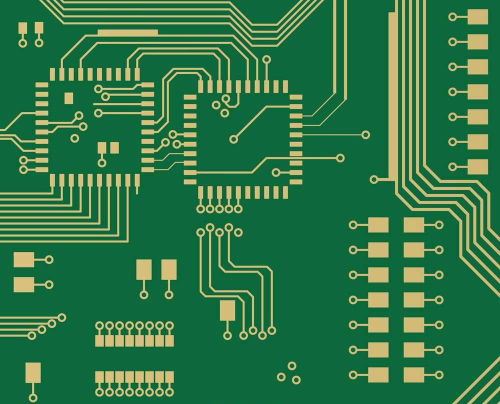
In PCBA turnkey processing, the solder mask is a very important coating material. It provides dielectric and mechanical shielding for the PCBA board during and after soldering and prevents solder from depositing in those areas. Generally, there are two types of solder mask materials commonly used in electronics manufacturing: liquid and dry film.
In PCBA and SMT assembly, solder mask ink is very important. Its main function is to protect the circuit board, prevent conductor tinning, prevent short circuits caused by moisture, prevent open circuits caused by improper contact during processing, and is one of the reasons that ensure the PCBA board can function properly in harsh environments. Below is a brief introduction to defective solder mask design in PCBA turnkey processing:
1. Connection between pads and through-holes: According to the principle, the trace connecting the mounting pads to the through-holes should be covered with solder mask.
2. Solder mask design between pads: Solder mask patterns and specifications should be designed according to the specific layout of component solder terminals. If an open-window solder mask is used between pads, a short circuit may occur during soldering. Designing individual solder mask isolation between pins prevents short circuits between pads during soldering.
3. Improper solder mask pattern size for components: Excessively large solder mask patterns can overlap and cause areas with no solder mask, especially when component spacing is too small.
4. Through-holes under components not covered by solder mask: Without solder mask on through-holes under components, solder on these holes after wave soldering may affect the reliability of IC soldering and may also cause short circuits or other defects in components.
The importance of PCBA drying and draining
What is Solder Mask?



SEND MESSAGE