
What is the main inspection of manual visual inspection during PCBA inspection?
2024-08-24
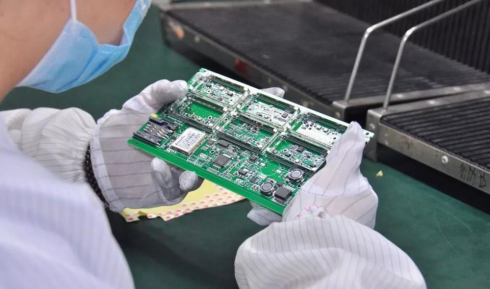
At present, manual visual inspection in the process of PCBA inspection is mainly through the naked eye or with the help of some relatively simple optical magnification instruments, manual visual inspection of PCB solder paste printing and solder joints, which is a method with less input and effective, for manufacturers with low process requirements, equipment and testing equipment imperfection, manual visual inspection has played an important role in improving the quality of assembly products.
Manual visual inspection includes: manual inspection of printed PCB, manual visual inspection of glue joints, manual visual inspection of solder joints and visual inspection of surface quality of printed PCB, etc.
Manual visual inspection is the first thing that needs to be done after solder paste printing, component placement, and soldering. The main test contents are as follows:
1. Solder paste printing
First of all, check whether the parameters of the solder paste printing machine are set correctly, the solder paste of the PCB is printed on the pad, whether the height of the solder paste is consistent or presents a "trapezoidal" shape, the edge of the solder paste should not have rounded corners or collapse into a pile of shapes, but it is allowed to have some peak-like shape caused by pulling up a small amount of solder paste when the steel plate is detached, if the solder paste is unevenly distributed, it is necessary to detect the solder paste on the scraper, whether it is insufficient or unevenly distributed, and it is also necessary to check the printed steel plate and other parameters. Finally, under a microscope, check whether the solder paste is shiny after printing.
2. Component placement
Before the first PCB with solder paste starts to place the components, confirm whether the rack is properly placed, whether the components are correct, and whether the machine is in the correct position before printing. After the first PCB is completed, check that each component is correctly placed and lightly pressed against the center of the paste, rather than just "placed" on top of the paste. If you can see a slight depression in the solder paste in the microscope, it means that it has been placed correctly. Whether all the components on the bill of materials (BOM) table are consistent with the components on the PCB, and whether all components that are sensitive to the positive and negative poles, such as diodes, tantalum electrolytic capacitors and ICs, are placed in the correct direction.
What material is a PCB board made of?
What are the special processes for PCB manufacturing ?



SEND MESSAGE