
To Ensure Good Copper Pour in PCB, These Points Cannot Be Overlooked!
2025-12-11
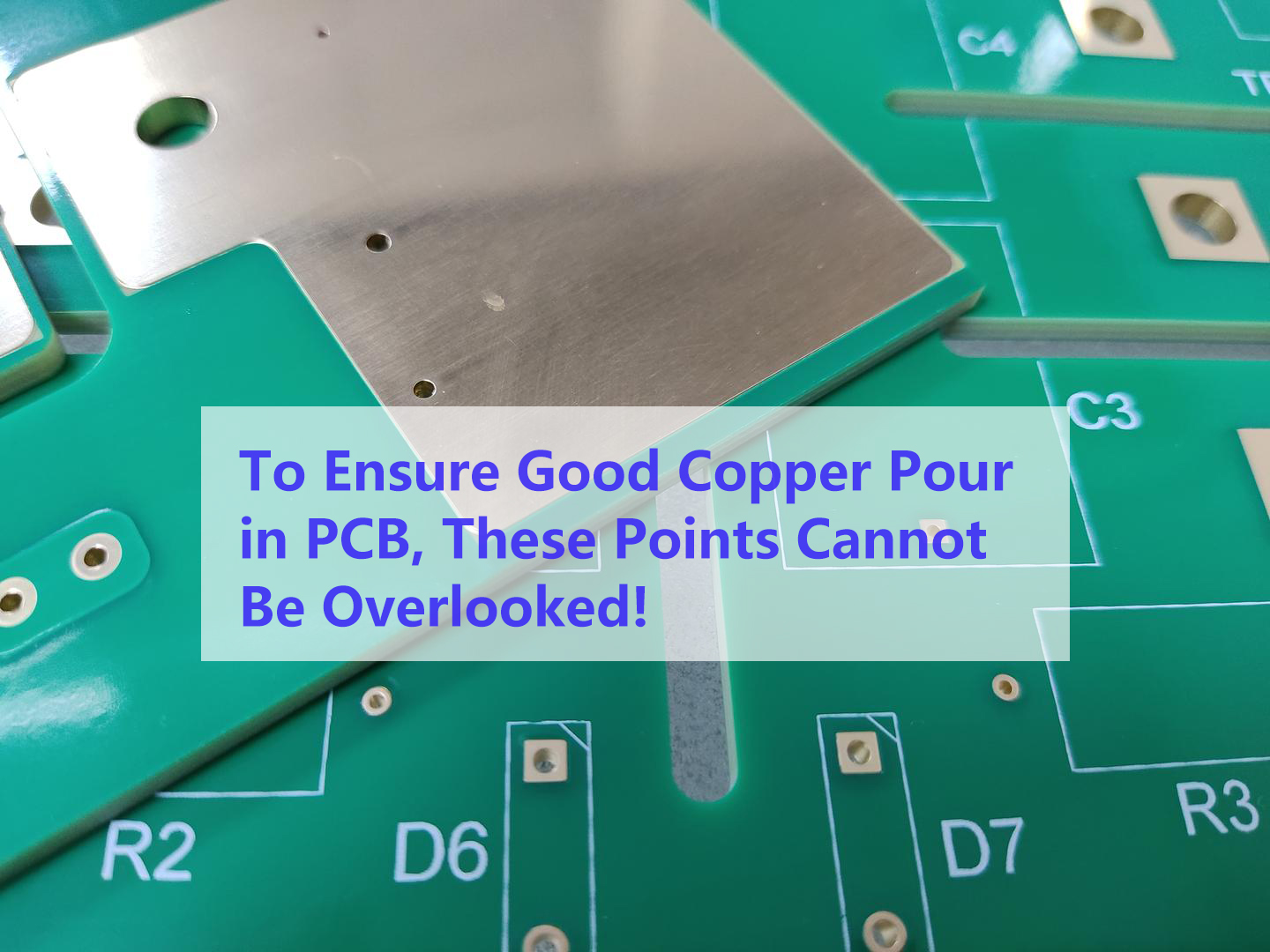
In high-speed PCB design, the handling of copper pour is crucial for ensuring signal integrity and electromagnetic compatibility. Today, professional PCBA manufacturer STG Electronic will explain the methods of copper pouring in high-speed PCB design.
Methods for properly handling copper pour in high-speed PCB design:
1. Differential Pair Copper Pour: For differential signals, ensure they have equal and opposite copper pours on adjacent layers. This helps improve signal immunity, reduce crosstalk, and enhance the quality of differential signals.
2. Ground Plane Copper Pour: In high-speed PCBs, the ground plane is critical. Adding a ground plane copper pour on every layer provides a good ground reference plane, reduces the inductance of the signal return path, and helps minimize interference caused by ground return currents.
3. Maintain Appropriate Copper Thickness: Copper thickness directly affects signal transmission characteristics. In high-speed design, thicker copper layers are typically chosen to reduce resistance and improve conductivity.
4. Avoid Exposed Copper Areas: Exposed copper areas can lead to electromagnetic interference, so it is essential to avoid them in the design. Ensure copper layers are fully enclosed, especially in high-frequency regions.
5. Control Interlayer Coupling of Copper Pour: In multi-layer board designs, carefully consider the coupling between different copper layers. Using appropriate interlayer spacing and meticulous planning of interlayer copper pour can help reduce interlayer coupling effects.
6. Avoid Sharp Copper Corners: Sharp copper corners may cause localized current concentration, leading to high-frequency losses and radiation. Using smoother copper shapes can mitigate this effect.
7. Consider Electromagnetic Shielding: In high-frequency environments, consider adding electromagnetic shielding layers to copper layers to improve electromagnetic compatibility and prevent mutual interference between radiation and sensitive components.
8. Use Simulation Tools for Verification: In the early stages of design, use simulation tools to verify the copper pour scheme and ensure it meets design requirements. This helps identify potential issues and make adjustments.
9. Pay Attention to Signal Routing Paths: Ensure signal routing paths are reasonable, avoiding excessively long or convoluted traces to reduce signal transmission delays and losses.
In high-speed PCB design, properly handling copper pour is a key step to ensure circuit performance and reliability. Through careful planning and simulation verification, issues related to signal integrity and electromagnetic compatibility can be minimized to the greatest extent.
If you need to learn more about PCB prototyping, SMT assembly, or PCBA processing, feel free to leave a message to get more technical knowledge!
The Explosion of the Charging Pile Industry: Uncovering How High-Quality PCBA Becomes the Key to Market Success
Unveiling the Mystery of Medical PCB Substrate Materials: Choosing the Wrong Material Can Be Fatal!



SEND MESSAGE