
Top 10 PCBA Industry Technology Trends in 2025: From High-Density Interconnect to AI-Powered Quality Inspection
2025-07-31
Top 10 PCBA Industry Technology Trends in 2025: From High-Density Interconnect to AI-Powered Quality Inspection
The Printed Circuit Board Assembly (PCBA) industry is undergoing a transformative phase, driven by rapid advancements in electronics manufacturing, artificial intelligence (AI), and material science. As we approach 2025, several key trends are shaping the future of PCB assembly, enabling higher performance, smarter manufacturing, and more reliable products.
The Printed Circuit Board Assembly (PCBA) industry is undergoing a transformative phase, driven by rapid advancements in electronics manufacturing, artificial intelligence (AI), and material science. As we approach 2025, several key trends are shaping the future of PCB assembly, enabling higher performance, smarter manufacturing, and more reliable products.
Here are the top 10 PCBA technology trends in 2025 that will redefine electronics manufacturing:
1. Ultra-High-Density Interconnect (HDI) PCBs
With the demand for miniaturization in consumer electronics, IoT, and medical devices, HDI PCBs are becoming the standard. Advanced laser drilling and stacked microvias allow for finer traces, higher component density, and improved signal integrity—critical for 5G, AI chips, and high-speed computing.
With the demand for miniaturization in consumer electronics, IoT, and medical devices, HDI PCBs are becoming the standard. Advanced laser drilling and stacked microvias allow for finer traces, higher component density, and improved signal integrity—critical for 5G, AI chips, and high-speed computing.
2. Embedded Components & 3D PCBA
Embedding passive and active components inside the PCB substrate reduces footprint, enhances electrical performance, and improves thermal management. 3D-printed electronics and additive manufacturing techniques are also enabling complex, multi-layer PCBA designs.
Embedding passive and active components inside the PCB substrate reduces footprint, enhances electrical performance, and improves thermal management. 3D-printed electronics and additive manufacturing techniques are also enabling complex, multi-layer PCBA designs.
3. AI-Driven Automated Optical Inspection (AOI)
AI-powered automated quality inspection is revolutionizing defect detection. Machine learning algorithms analyze solder joints, component placement, and micro-defects with >99% accuracy, reducing false positives and speeding up production.
AI-powered automated quality inspection is revolutionizing defect detection. Machine learning algorithms analyze solder joints, component placement, and micro-defects with >99% accuracy, reducing false positives and speeding up production.
4. Advanced Materials for High-Frequency & Thermal Management
New low-loss dielectric materials (e.g., PTFE, ceramic-filled laminates) support mmWave and terahertz frequencies for 6G and radar systems. Meanwhile, graphene-enhanced thermal substrates help dissipate heat in high-power applications like EVs and data centers.
New low-loss dielectric materials (e.g., PTFE, ceramic-filled laminates) support mmWave and terahertz frequencies for 6G and radar systems. Meanwhile, graphene-enhanced thermal substrates help dissipate heat in high-power applications like EVs and data centers.
5. Smart Manufacturing with Digital Twins
Digital twin technology creates virtual replicas of PCBA production lines, enabling real-time monitoring, predictive maintenance, and process optimization. This reduces downtime and improves yield rates in smart factories.
Digital twin technology creates virtual replicas of PCBA production lines, enabling real-time monitoring, predictive maintenance, and process optimization. This reduces downtime and improves yield rates in smart factories.
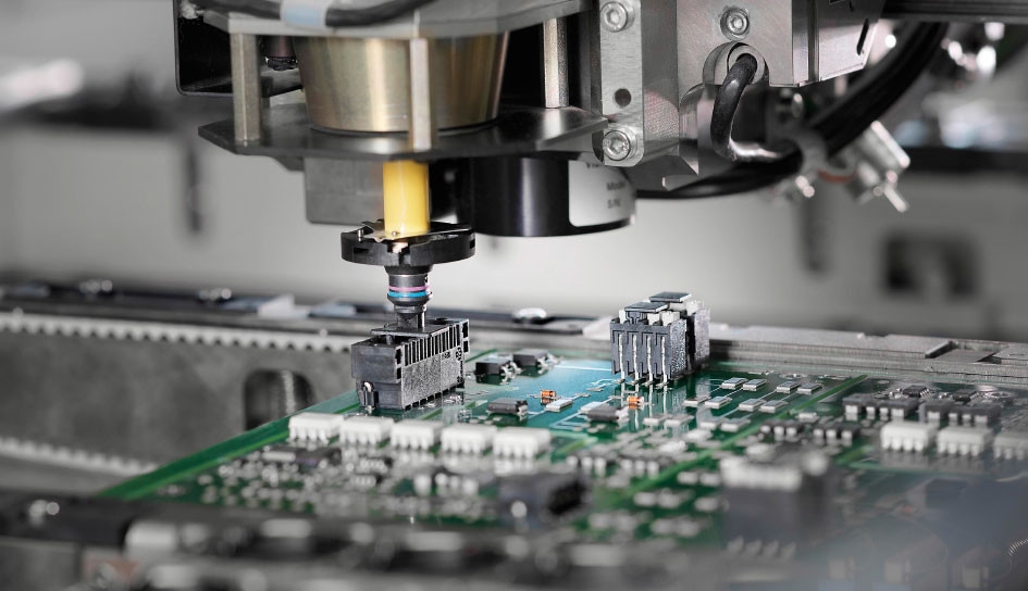
6. Robotic Soldering & Precision Assembly
Collaborative robots (cobots) equipped with AI vision systems are enhancing precision soldering, especially for micro-BGA and 01005 components. Self-learning algorithms adapt to variations in board warpage and solder paste deposition.
Collaborative robots (cobots) equipped with AI vision systems are enhancing precision soldering, especially for micro-BGA and 01005 components. Self-learning algorithms adapt to variations in board warpage and solder paste deposition.
7. Sustainable & Eco-Friendly PCBA
With stricter RoHS 3.0 and REACH regulations, manufacturers are adopting lead-free solders, halogen-free substrates, and biodegradable PCBs. Recycling rare metals from e-waste is also gaining traction.
With stricter RoHS 3.0 and REACH regulations, manufacturers are adopting lead-free solders, halogen-free substrates, and biodegradable PCBs. Recycling rare metals from e-waste is also gaining traction.
8. Edge AI Integration in PCBA
Embedded AI accelerators (e.g., NPUs, TPUs) are being integrated directly into PCBAs for real-time data processing in autonomous vehicles, smart sensors, and Industry 4.0 applications.
Embedded AI accelerators (e.g., NPUs, TPUs) are being integrated directly into PCBAs for real-time data processing in autonomous vehicles, smart sensors, and Industry 4.0 applications.
9. Flexible & Stretchable PCBs for Wearables
Next-gen flexible hybrid electronics (FHE) enable bendable, stretchable, and even self-healing PCBs, ideal for medical wearables, foldable smartphones, and soft robotics.
Next-gen flexible hybrid electronics (FHE) enable bendable, stretchable, and even self-healing PCBs, ideal for medical wearables, foldable smartphones, and soft robotics.
10. Blockchain for PCBA Supply Chain Security
To combat counterfeit components, blockchain-based traceability ensures authentic sourcing of ICs, resistors, and capacitors—critical for aerospace, defense, and medical electronics.
To combat counterfeit components, blockchain-based traceability ensures authentic sourcing of ICs, resistors, and capacitors—critical for aerospace, defense, and medical electronics.
Conclusion: The Future of PCBA is Smarter, Faster, and More Connected
By 2025, the PCBA industry will be defined by AI-enhanced manufacturing, ultra-compact designs, and sustainable practices. Companies that adopt these trends early will lead in innovation, efficiency, and reliability—paving the way for the next generation of smart electronics.
By 2025, the PCBA industry will be defined by AI-enhanced manufacturing, ultra-compact designs, and sustainable practices. Companies that adopt these trends early will lead in innovation, efficiency, and reliability—paving the way for the next generation of smart electronics.
Why PCBA Processing is Critical for Communications and IoT
Japan's PCB Giant Meiko Commences Production at Vietnam's 5th Factory; $350M Phase 2 Project Underway



SEND MESSAGE