
Must-See for SMT Prototyping! 5 Core Quality Control Points, Full Process Breakdown from Materials to Craftsmanship
2025-12-15
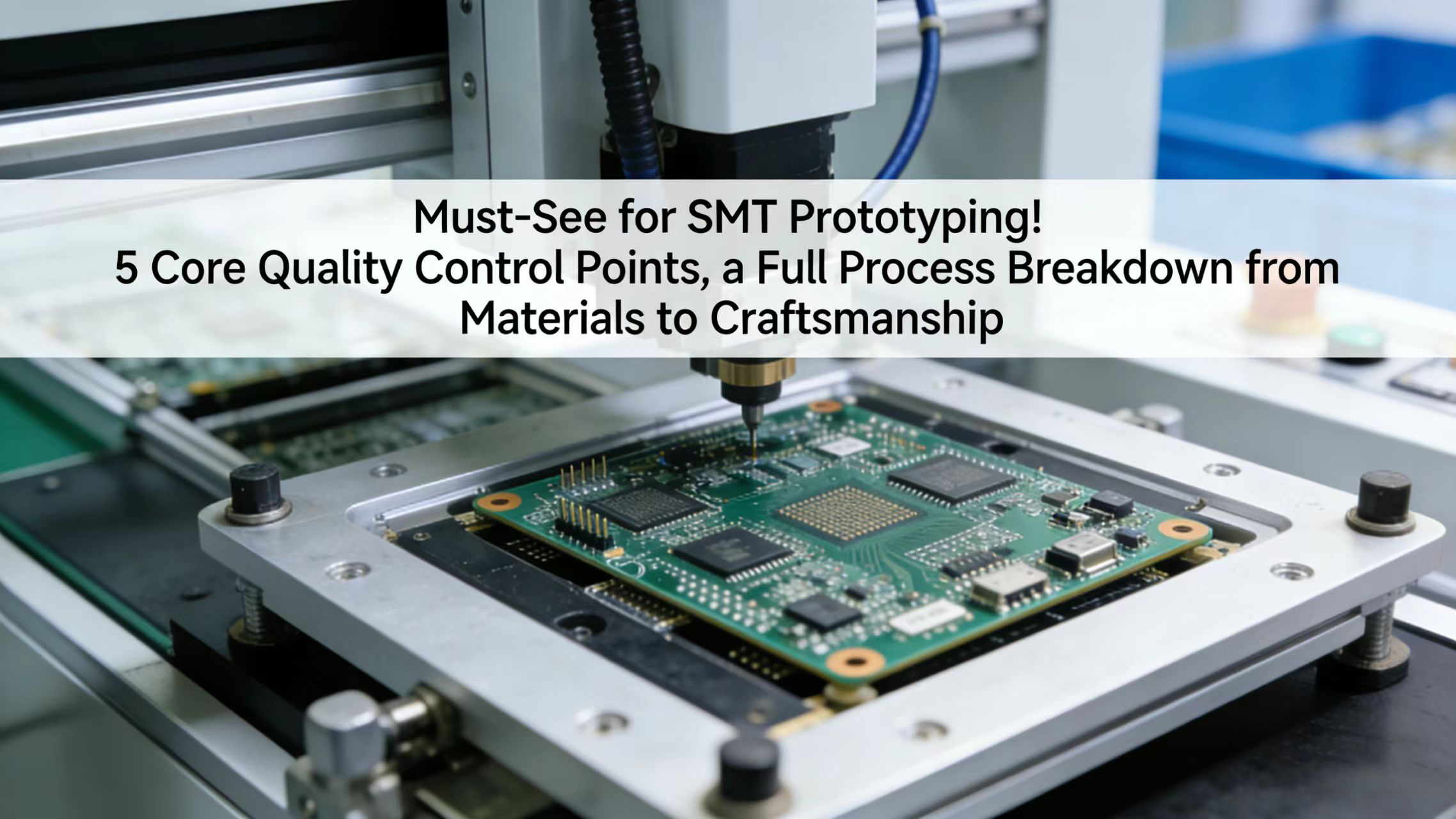
Analysis of 5 Core Quality Control Requirements for SMT Prototyping
1. Three-Level Component Verification System: Ensuring Quality from the Source
Traceable Sourcing: All components in the BOM must be 100% sourced through original manufacturers to avoid using refurbished or counterfeit parts. For example, implement unique code tracing for high-value IC chips, ensuring they match supplier batch records.
Composition Testing: Perform X-ray fluorescence analysis on key materials (e.g., solder paste, PCB substrate) to verify composition ratios comply with RoHS standards. For example, checking if deviations in tin, silver, and copper content in solder paste are within ±0.5%.
Environmental Control: Sensitive components (e.g., BGA, QFN) must be stored in constant temperature/humidity warehouses (23±2℃ / 40-60% RH) to prevent moisture absorption and resulting solder voids. For instance, BGA devices must be placed within 24 hours after opening, otherwise requiring re-baking for moisture removal.
Composition Testing: Perform X-ray fluorescence analysis on key materials (e.g., solder paste, PCB substrate) to verify composition ratios comply with RoHS standards. For example, checking if deviations in tin, silver, and copper content in solder paste are within ±0.5%.
Environmental Control: Sensitive components (e.g., BGA, QFN) must be stored in constant temperature/humidity warehouses (23±2℃ / 40-60% RH) to prevent moisture absorption and resulting solder voids. For instance, BGA devices must be placed within 24 hours after opening, otherwise requiring re-baking for moisture removal.
2. Process Parameter Pre-Verification: Precision Control for Every Step
Stencil Design: Use 3D simulation software to optimize stencil aperture design, ensuring uniform solder paste printing thickness. For example, step stencils are recommended for 0201 components, locally thickened by 0.03mm to compensate solder paste volume.
SPI Inspection: Implement online solder paste thickness inspection (3σ control), ensuring printing deviation is less than 15% of the pad width. For instance, if the pad width is 0.3mm, the solder paste thickness deviation must be controlled within ±0.045mm.
Placement Accuracy: Calibrate the pick-and-place machine via a dual vision alignment system, controlling the placement offset of 0201 components to within ±25μm (per IPC-9850 standard). For example, using a laser interferometer to verify the equipment coordinate system, ensuring X/Y/Z axis mechanical deviation ≤ 15μm.
SPI Inspection: Implement online solder paste thickness inspection (3σ control), ensuring printing deviation is less than 15% of the pad width. For instance, if the pad width is 0.3mm, the solder paste thickness deviation must be controlled within ±0.045mm.
Placement Accuracy: Calibrate the pick-and-place machine via a dual vision alignment system, controlling the placement offset of 0201 components to within ±25μm (per IPC-9850 standard). For example, using a laser interferometer to verify the equipment coordinate system, ensuring X/Y/Z axis mechanical deviation ≤ 15μm.
3. Dual Process Monitoring: Real-Time Feedback & Intelligent Comparison
Reflow Oven Zone Monitoring: Equip a 10-zone reflow oven, using thermocouples to collect real-time PCB surface temperatures, ensuring peak temperature fluctuation ≤ ±5℃. For example, setting a peak temperature of 235-245℃ for lead-free solder (SnAgCu), maintained for 40-60 seconds.
First-Article Intelligent Comparison: Utilize AOI (Automated Optical Inspection) to perform pixel-level comparison between the first article sample and Gerber files, automatically identifying defects like solder joint offset, component polarity errors. For example, enabling 3D inspection mode for BGA devices, using multi-angle light source compensation to eliminate shadow interference.
100% AOI Inspection: Perform 100% AOI inspection on post-reflow boards, focusing on 11 solder joint criteria (e.g., wetting angle, bridging, cold solder). For example, requiring a solder joint wetting angle ≥40°, and freedom from defects like bridging or solder balls.
First-Article Intelligent Comparison: Utilize AOI (Automated Optical Inspection) to perform pixel-level comparison between the first article sample and Gerber files, automatically identifying defects like solder joint offset, component polarity errors. For example, enabling 3D inspection mode for BGA devices, using multi-angle light source compensation to eliminate shadow interference.
100% AOI Inspection: Perform 100% AOI inspection on post-reflow boards, focusing on 11 solder joint criteria (e.g., wetting angle, bridging, cold solder). For example, requiring a solder joint wetting angle ≥40°, and freedom from defects like bridging or solder balls.
4. Data-Driven Quality Traceability: Closed-Loop Full-Process Management
Independent Process Records: Create electronic process records for each prototyping batch, documenting key parameters like stencil tension, placement pressure, reflow profile. For example, a stencil usage log must record that the stencil is mandatorily scrapped when tension falls to 28N/cm2.
Cloud Data Storage: Upload SPI and AOI inspection data to cloud servers, ensuring a traceability period of ≥10 years. For instance, using SPC (Statistical Process Control) systems to analyze solder paste thickness fluctuation trends and provide early warnings for process drift.
SPC Analysis of Anomalies: Automatically generate control charts for non-conforming points during production to identify special cause variation. For example, triggering a process parameter adjustment procedure if 7 consecutive points appear on the same side of the centerline.
Cloud Data Storage: Upload SPI and AOI inspection data to cloud servers, ensuring a traceability period of ≥10 years. For instance, using SPC (Statistical Process Control) systems to analyze solder paste thickness fluctuation trends and provide early warnings for process drift.
SPC Analysis of Anomalies: Automatically generate control charts for non-conforming points during production to identify special cause variation. For example, triggering a process parameter adjustment procedure if 7 consecutive points appear on the same side of the centerline.
5. Enhanced Reliability Testing: Validation Under Simulated Extreme Conditions
Thermal Cycling Test: Perform temperature cycling tests from -40℃ to 125℃ for medical/automotive electronics to verify solder joint thermal fatigue life. For example, after 1000 cycles, requiring the solder joint IMC (Intermetallic Compound) layer thickness to be ≤5μm.
Vibration Test: Use a 5-500Hz sine sweep vibration table to simulate vibration environments during product transportation or use. For example, for automotive electronics, requiring vibration acceleration ≤5G, with no component detachment or solder joint cracking.
Cross-Sectional (Microsection) Analysis: Perform destructive testing on critical solder joints, using microscopes to observe IMC layer uniformity. For example, requiring a continuous, void-free IMC layer between BGA solder balls and PCB pads, with thickness deviation ≤20%.
Vibration Test: Use a 5-500Hz sine sweep vibration table to simulate vibration environments during product transportation or use. For example, for automotive electronics, requiring vibration acceleration ≤5G, with no component detachment or solder joint cracking.
Cross-Sectional (Microsection) Analysis: Perform destructive testing on critical solder joints, using microscopes to observe IMC layer uniformity. For example, requiring a continuous, void-free IMC layer between BGA solder balls and PCB pads, with thickness deviation ≤20%.
Quality control during the SMT prototyping stage should be data-driven at its core. A closed-loop quality management system is constructed through five key phases: three-level component verification, process parameter pre-calibration, dual-process monitoring, full-process traceability, and enhanced reliability testing. For example, a high-end medical device manufacturer, by implementing the above plan, increased their prototyping yield from 85% to 99.2%, simultaneously reducing customer complaint rates to below 0.3%, significantly shortening the product time-to-market.
If you require PCBA Prototyping, PCBA Contract Manufacturing, or PCBA Assembly, please feel free to send us an inquiry for a quotation.
[Urgent Alert] Component Shortage Crisis Looming! Prices of These Core PCBA Components May Soar at Any Moment!
The Explosion of the Charging Pile Industry: Uncovering How High-Quality PCBA Becomes the Key to Market Success



SEND MESSAGE