
5-Day PCBA Prototyping: How STG Electronic Accelerates Your Time-to-Market
2026-04-16
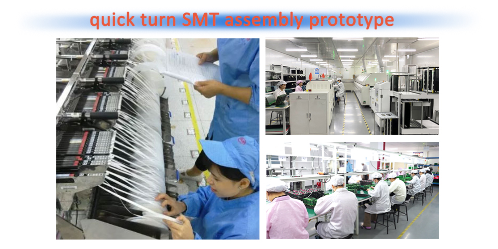
In product development, every day counts. A week lost in PCBA prototyping can push your entire launch behind schedule.
At STG Electronic Co., Ltd, we’ve helped global clients cut prototyping lead times by over 50% since 2002. Here’s how.
The Traditional Problem
Step Typical Lead Time
PCB fabrication 7–10 days
Component sourcing 5–15 days
SMT assembly 5–7 days
Testing 2–3 days
Total 19–35 days
Most factories treat each step separately. Delays pile up.
STG’s Integrated Approach
We combine all steps under one roof with one project manager:
Step STG Lead Time
PCB + sourcing + assembly + testing 5–7 days
PCB + sourcing + assembly + testing 5–7 days
No handoff delays. No communication gaps.

What Makes 5-Day Prototyping Possible?
- In-house PCB fabrication – No waiting for outside suppliers
- Component inventory – Common parts stocked for quick pick
- Dedicated prototype SMT line – No queue behind production orders
- Same-day DFM review – Issues caught before manufacturing starts
Quality Is Never Rushed
- Fast doesn't mean fragile. Every prototype undergoes:
- AOI inspection – Solder joint verification
- X-ray (if BGA) – Hidden defect detection
- Functional testing – Board works as designed
Why Choose STG Electronic?
- 24 years of PCBA experience
- 500+ prototypes delivered to global clients annually
- ISO9001:2015 certified
- X-ray + AOI for 100% BGA inspection
Ready to Cut Your Prototyping Lead Time?
Send us your Gerber files and BOM. We’ll respond with a free DFM report and a firm delivery date—within 24 hours.
Fast. Reliable. No surprises.
Through-Hole vs SMT Assembly: Which One Fits Your Project?
8-Layer PCB Impedance Control: Why It Matters for Your High-Speed Design



SEND MESSAGE