
3D-Printed PCB: Revolutionizing Prototype Manufacturing for More Efficient and Faster Custom PCBA
2025-12-08
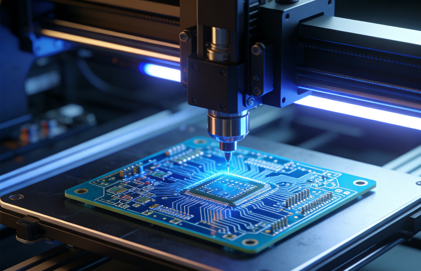
In today's fast-paced landscape of hardware innovation, 3D-printed PCB technology is revolutionizing electronic prototype development and custom PCBA (Printed Circuit Board Assembly) with its unique advantages. By enabling a fully digital workflow, it seamlessly bridges the gap between design and physical realization, elevating both "speed" and "flexibility" to unprecedented levels.
Core Advantages: Ultimate Simplification, Speed First
Unlike traditional PCB manufacturing, which relies on complex processes such as masking, etching, and outsourcing, 3D printing PCBs is fundamentally rooted in additive manufacturing. Design files can directly drive the printer to build circuits layer by layer, truly achieving "design-to-production" in one step. This approach eliminates long lead times for prototyping and avoids the need for tooling, such as custom stencils.
Unlike traditional PCB manufacturing, which relies on complex processes such as masking, etching, and outsourcing, 3D printing PCBs is fundamentally rooted in additive manufacturing. Design files can directly drive the printer to build circuits layer by layer, truly achieving "design-to-production" in one step. This approach eliminates long lead times for prototyping and avoids the need for tooling, such as custom stencils.
Even more noteworthy, advanced 3D printing solutions can directly print solder paste or conductive inks and integrate component placement and soldering processes. This means the time from concept to a functional PCBA prototype can be reduced to just hours or even less. For R&D teams, makers, educational institutions, and companies that require rapid design validation, this translates not only to time savings but also to a significantly accelerated innovation cycle.
Current Limitations and Future Outlook
Currently, this technology is better suited for designs with limited complexity, such as single or double-layer boards, and material costs remain higher compared to traditional mass production. This clarifies its role: rather than replacing conventional large-scale manufacturing, it serves as an ideal tool for prototype verification, small-batch customization, urgent repairs, and specialized education.
As functional electronic materials (such as inks with higher conductivity and better thermal stability) and printing precision continue to improve, the capabilities of 3D-printed PCBs are steadily expanding. In the future, the technology is expected to handle more complex circuit layouts and even embedded components.
Conclusion
In summary, 3D-printed PCBs offer a highly autonomous, rapidly responsive, and flexible manufacturing pathway. They significantly lower the entry barriers for hardware innovation and reduce dependence on complex supply chains, allowing ideas to be tested in reality much faster. In an era that prioritizes agile development, this technology has become an indispensable accelerator for engineers and innovators, consistently driving the efficient transformation from concept to product.
In summary, 3D-printed PCBs offer a highly autonomous, rapidly responsive, and flexible manufacturing pathway. They significantly lower the entry barriers for hardware innovation and reduce dependence on complex supply chains, allowing ideas to be tested in reality much faster. In an era that prioritizes agile development, this technology has become an indispensable accelerator for engineers and innovators, consistently driving the efficient transformation from concept to product.
Little Tricks for PCBA Cost Saving
The Application of PCBA Products in the Medical Field



SEND MESSAGE