
PCBA Assembly Process: 6 Key Steps from Solder Paste to Functional Testing
2026-04-29

Understanding the PCBA assembly process helps you identify quality issues and communicate better with your manufacturer.
At STG Electronic Co., Ltd, we've followed a proven 6-step workflow for global clients since 2002. Here's what happens after you send your files.
The 6-Step Process
Step What Happens Quality Check
1. Solder Paste Printing Paste applied to PCB pads via stencil SPI (Solder Paste Inspection)
2. SMT Assembly Components placed on paste AOI after placement
3. Reflow Soldering Board heated to melt solder paste Temperature profile logging
4. Wave Soldering Through-hole components soldered (if present) Visual + AOI
5. Inspection Defect detection AOI, X-ray, or manual
6. Functional Testing Board powered on to verify operation Pass/Fail record
Why Each Step Matters
Step 1 – Solder Paste Printing
Too little paste = weak joint. Too much = short circuit. SPI catches this before placement.
Step 2 – SMT Assembly
Speed matters, but accuracy matters more. STG uses high-precision mounters for 01005 components.
Speed matters, but accuracy matters more. STG uses high-precision mounters for 01005 components.
Step 3 – Reflow Soldering
The temperature curve must match your solder paste and components. We verify every profile.
The temperature curve must match your solder paste and components. We verify every profile.

Step 4 – Wave Soldering
For through-hole components (connectors, switches, large capacitors), SMT alone won't work. The board travels over a molten solder wave that solders all exposed pins simultaneously.
For through-hole components (connectors, switches, large capacitors), SMT alone won't work. The board travels over a molten solder wave that solders all exposed pins simultaneously.
The wave soldering sub-steps:
- Flux application – Cleans surfaces for better solder adhesion
- Pre-heating – Activates flux and reduces thermal shock
- Solder wave – Board passes over molten solder at 250–260°C
- Cooling – Solidifies joints cleanly
Common defects we check: Solder bridges, insufficient fill, voids. Every wave-soldered board gets post-wave AOI.

Step 5 – Inspection (AOI + X-ray)
AOI sees surface defects. X-ray sees hidden BGA solder joints.
AOI sees surface defects. X-ray sees hidden BGA solder joints.
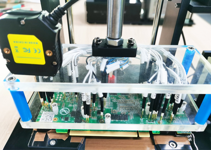
Step 6 – Functional Testing
The final gate. We power your board and confirm it works as designed.
The final gate. We power your board and confirm it works as designed.

Why Choose STG Electronic?
- 24 years of PCBA experience
- In-house testing – SPI, AOI, X-ray, functional test
- ISO9001:2015 certified
Ready to See Your Board Built Right?
Send us your Gerber files and BOM. We'll respond with a process review and a quote—within 24 hours.
Holiday Notice: Labor Day 2026
Rogers High Density Interconnector PCB Selection Guide: Differences Between RO4003, RO4350B, and RO5880
Related Article



SEND MESSAGE