
Application of HDI Boards in HDI PCB Field: How Laser Blind Vias Improve Signal Integrity
2026-04-24
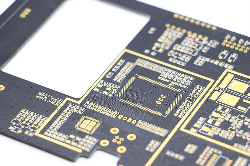
As applications such as 5G communications, millimeter-wave radar, and high-speed optical modules evolve toward higher frequency bands, PCB signal integrity has become a bottleneck for system performance. Traditional through-hole structures generate significant parasitic capacitance and stub effects at high frequencies, severely degrading signal quality. The combination of HDI boards and laser blind via technology is the key solution to this problem.

STG Electronic Co., Ltd has specialized in high-frequency boards for over 20 years, supporting mass production of 2- to 36-layer HDI boards. We master laser blind via + copper plating fill processes to ensure high-fidelity transmission of high-frequency signals.
1. Why Are HDI Boards and Laser Blind Vias Needed in High-Frequency Applications?
Traditional Through-Hole Issues Impact at High Frequencies HDI + Laser Blind Via Solution
Long via stub Signal reflection and resonance, poor eye diagram Blind vias have no stub, shortest signal path
Large parasitic capacitance Lowers characteristic impedance, causes impedance discontinuity Small blind via aperture (≤0.1mm), low parasitic effect
Occupies routing space Limits fan-out of high-density pin devices (e.g., 0.4mm BGA) Microvias/buried vias free up multilayer routing area
Increased layer count Higher insertion loss and manufacturing cost ELIC (Every Layer Interconnect) reduces through-hole count
Long via stub Signal reflection and resonance, poor eye diagram Blind vias have no stub, shortest signal path
Large parasitic capacitance Lowers characteristic impedance, causes impedance discontinuity Small blind via aperture (≤0.1mm), low parasitic effect
Occupies routing space Limits fan-out of high-density pin devices (e.g., 0.4mm BGA) Microvias/buried vias free up multilayer routing area
Increased layer count Higher insertion loss and manufacturing cost ELIC (Every Layer Interconnect) reduces through-hole count
Core Conclusion: In frequency bands ≥10GHz, laser blind via HDI boards are a necessary process for achieving signal integrity — not an optional choice.
2. How Does Laser Blind Via Technology Improve Signal Integrity?
Technical Mechanism Contribution to Signal Integrity
Eliminates stub No residual via section, eliminates frequency notch effect, insertion loss reduced by 0.5-1dB @ 28GHz
Reduces parasitic capacitance Pad diameter ≤0.25mm, parasitic capacitance reduced by ~70%, smaller impedance fluctuation
Shortens signal path Blind vias go directly from outer layer to inner layer, reduces via count, lowers delay mismatch
Optimizes return path More flexible design for adjacent ground vias, reduces loop inductance, minimizes EMI
Eliminates stub No residual via section, eliminates frequency notch effect, insertion loss reduced by 0.5-1dB @ 28GHz
Reduces parasitic capacitance Pad diameter ≤0.25mm, parasitic capacitance reduced by ~70%, smaller impedance fluctuation
Shortens signal path Blind vias go directly from outer layer to inner layer, reduces via count, lowers delay mismatch
Optimizes return path More flexible design for adjacent ground vias, reduces loop inductance, minimizes EMI
3. STG Electronic HDI Board Process Capabilities
Process Parameter STG Capability
Maximum Layers 36 layers
Minimum Laser Blind Via Aperture 0.075mm
Minimum Mechanical Buried Via Aperture 0.15mm
Minimum Line Width/Space 0.075mm / 0.075mm
Blind Via Copper Fill Copper plating fill, dimple ≤15μm
Stackup Types 1-Step, 2-Step, 3-Step, Every Layer Interconnect (ELIC)
Material Compatibility Rogers, Taconic, F4B, FR-4 hybrid lamination + HDI
Maximum Layers 36 layers
Minimum Laser Blind Via Aperture 0.075mm
Minimum Mechanical Buried Via Aperture 0.15mm
Minimum Line Width/Space 0.075mm / 0.075mm
Blind Via Copper Fill Copper plating fill, dimple ≤15μm
Stackup Types 1-Step, 2-Step, 3-Step, Every Layer Interconnect (ELIC)
Material Compatibility Rogers, Taconic, F4B, FR-4 hybrid lamination + HDI
The above capabilities have been applied to high-frequency projects such as 77G radar antenna boards, 400G optical module sub-boards, and phased array T/R modules.
4. Application Case: 28GHz Millimeter-Wave Transceiver Module
Project Parameter Details
Layer Count/Stackup 10 layers, 2-Step blind/buried via structure (1-3, 3-8, 8-10)
Material Rogers RO4835 + FR-4 hybrid lamination
Minimum Blind Via 0.1mm (laser)
BGA Pitch 0.5mm
Insertion Loss Requirement ≤0.3dB/cm @ 28GHz
Layer Count/Stackup 10 layers, 2-Step blind/buried via structure (1-3, 3-8, 8-10)
Material Rogers RO4835 + FR-4 hybrid lamination
Minimum Blind Via 0.1mm (laser)
BGA Pitch 0.5mm
Insertion Loss Requirement ≤0.3dB/cm @ 28GHz
Result: Blind via stubs completely eliminated. Measured insertion loss of 0.28dB/cm. Impedance controlled at 50Ω ±4%. Customer has entered small-batch production.
In the High density interconnect PCB field, HDI board + laser blind via is the core technical path to achieving signal integrity. With 15+ years of high-frequency experience and full-process HDI capabilities, STG Electronic provides highly reliable interconnect solutions for your 5G, millimeter-wave, and optical module projects.
Rogers High Density Interconnector PCB Selection Guide: Differences Between RO4003, RO4350B, and RO5880
What Information Is Needed to Produce High Density Interconnector Circuit Boards?
Related Article



SEND MESSAGE