


3D-Printed PCB, Custom PCBA, More Efficient, Faster
3D-Printed PCB Custom PCBA
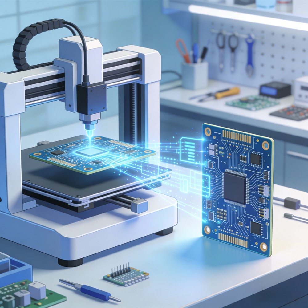
3D-printed PCBs are revolutionizing electronic prototyping, bringing unprecedented speed and flexibility to customized PCBAs. Their core advantage lies in significantly simplifying the production process: the complex steps of traditional manufacturing, such as mask making, etching, and outsourcing, are entirely eliminated, allowing design files to be instantly converted into physical circuit boards, achieving 'design-to-production.' At the same time, it eliminates the need for custom stencils, supports direct printing of solder paste, and completes component mounting and soldering, saving even more time from design to finished soldered product, making it especially suitable for rapid iteration and prototype testing.
Quantity
3D-Printed PCB Rapid Prototyping Solution
Print Now, Test Now
Our 3D-printed PCB solution is designed specifically for electronic prototype development and fast custom PCBA. Skip the long wait times of traditional manufacturing and transform your ideas into testable circuit boards in just hours.
🚀 Unmatched Speed
Traditional Process: Design → Order → Manufacturing → Etching → Outsourcing (7-15 days)
Traditional Process: Design → Order → Manufacturing → Etching → Outsourcing (7-15 days)
3D Printing Process: Design → Print → Test (As fast as same-day completion)
Save up to 90% in time, ideal for urgent projects and rapid iterations
🛠️ Simplified Workflow
No complex processes like masking, etching, or outsourcing
No complex processes like masking, etching, or outsourcing
Eliminates the need for custom stencils; solder paste is printed directly
Design files translate directly into physical boards—true"design-to-production"
💡 Flexibility and Autonomy
Production starts from just 1 piece—no minimum order quantity
Production starts from just 1 piece—no minimum order quantity
Supports real-time modifications and immediate printing
Can be done in labs or offices, reducing supply chain dependency
Technical Specifications
Item Specifications
Supported Layers Single-layer, Double-layer
Base Material Specialized 3D-printed electronic materials (engineering-grade polymer substrate)
Min. Line Width/Spacing 0.3mm / 0.3mm
Max. Printing Size 200mm × 200mm
Conductive Material Nano-silver conductive ink, low-temperature solder paste
Integrated Process Supports direct solder paste printing + component placement + soldering
Typical Delivery Time 4-8 hours (after design confirmation)
Ideal Use Cases
🔬 R&D and Prototype Validation
Functional verification prototypes
Concept testing circuits
Iterative design optimization
🎓 Education and Research
Electronics lab experiments
Electronics lab experiments
Student project development
Rapid implementation of research projects
🏭 Small-Batch Trial Production
Market testing products
Market testing products
Customized small-batch orders
Process validation samples
⚡ Urgent Needs
Quick fixes for design errors
Quick fixes for design errors
Emergency spare part production
On-site technical support
Comparison with Traditional PCB Manufacturing
Comparison Factor 3D-Printed PCB Traditional PCB
Prototyping Cycle Hours 3-7 days
Minimum Order Quantity 1 piece Typically 5-10 pieces
Stencil Requirement Not required Custom stencil needed
Design Flexibility Real-time modifications Requires re-manufacturing for changes
Complex Circuit Support Suitable for simple designs Suitable for complex multi-layer boards
Per-Unit Cost Higher Extremely low for bulk orders
Process Workflow

Technology Development Roadmap
We are continuously investing in R&D to deliver:
✅ Already Achieved: Single/double-layer board rapid manufacturing
🔄 In Development: 4-layer board technology (expected Q4 release)
📅 Planned: Embedded component printing, higher-precision conductive materials
Frequently Asked Questions
Q: How reliable are 3D-printed PCB?
A: Fully reliable for prototype validation and short-term testing. Conductivity meets the requirements of most low-frequency and digital circuits.
Q: What file formats are supported?
A: Gerber, .brd, .sch, and native formats from common EDA software.
A: Gerber, .brd, .sch, and native formats from common EDA software.
Q: How long can soldered circuits function?
A: Under normal conditions, they remain stable for several months—sufficient for most testing and validation cycles.
A: Under normal conditions, they remain stable for several months—sufficient for most testing and validation cycles.
Q: Do you offer component placement services?
A: Yes, we provide end-to-end services from printing to soldering.
A: Yes, we provide end-to-end services from printing to soldering.