The Complete Guide to Printed Circuit Board (PCB) Manufacturing
Introduction
Printed Circuit Boards (PCBs) are the backbone of modern electronics, providing mechanical support and electrical connections for components in devices ranging from smartphones to industrial machinery. The PCB manufacturing process involves multiple precise steps to ensure reliability, performance, and durability. This article explores the key stages of PCB production, from design to final assembly.
1. PCB Design & Engineering
Before manufacturing begins, engineers create a PCB layout using Electronic Design Automation (EDA) software such as Altium Designer, KiCad, or Cadence OrCAD. Key considerations include:
- Schematic Design – Defining circuit connections.
- Layer Stackup – Deciding the number of copper layers (single-sided, double-sided, or multilayer).
- Component Placement – Optimizing signal integrity and thermal management.
- Design Rule Check (DRC) – Ensuring manufacturability by avoiding errors like short circuits or insufficient spacing.
Once the design is finalized, Gerber files (industry-standard PCB blueprints) are generated for fabrication.
2. PCB Fabrication Process
A. Substrate Preparation
The base material, typically FR4 (fiberglass-reinforced epoxy laminate), is cut into panels. For high-frequency applications, materials like Rogers or PTFE may be used.
B. Copper Patterning (Photolithography)
- Copper Lamination – A thin copper layer is bonded to the substrate.
- Photoresist Application – A light-sensitive chemical is applied.
- UV Exposure & Etching – The PCB design is transferred using UV light, and unwanted copper is chemically etched away.
C. Drilling & Plating
- Mechanical Drilling – Holes for vias and component leads are drilled.
- Electroless Copper Deposition – A thin conductive layer is added to hole walls for electrical connectivity.
D. Solder Mask & Silkscreen
- Solder Mask Application – A protective green (or other colored) coating prevents short circuits.
- Silkscreen Printing – Component labels, logos, and identifiers are printed for assembly.
E. Surface Finish
To protect exposed copper and improve solderability, finishes like:
- HASL (Hot Air Solder Leveling)
- ENIG (Electroless Nickel Immersion Gold)
- OSP (Organic Solderability Preservative)
are applied.
3. PCB Assembly (PCBA)
After fabrication, components are mounted via:
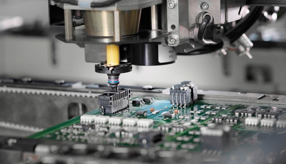
- Surface Mount Technology (SMT) – Automated pick-and-place machines install tiny components.
- Through-Hole Technology (THT) – Larger components are inserted into drilled holes and soldered.
- Reflow & Wave Soldering – Heat processes create permanent connections.
4. Testing & Quality Control
To ensure functionality, PCBs undergo:
- Automated Optical Inspection (AOI) – Checks for soldering defects.
- In-Circuit Testing (ICT) – Verifies electrical performance.
- Functional Testing – Ensures the board operates as intended.
5. Applications of PCBs
PCBs are used in nearly every electronic device, including:
- Consumer Electronics (Smartphones, Laptops)
- Automotive Systems (ECUs, Infotainment)
- Medical Devices (Imaging Equipment, Wearables)
- Industrial Automation (Robotics, Control Systems)
Conclusion
PCB manufacturing is a complex yet highly optimized process that balances precision, efficiency, and innovation. As technology advances, trends like HDI (High-Density Interconnect) PCBs, flexible circuits, and IoT-optimized designs continue to push the boundaries of electronics.
Whether for prototyping or mass production, understanding PCB manufacturing helps engineers and businesses deliver reliable, high-performance electronic solutions.
Would you like a more detailed section on any specific PCB technology (e.g., HDI, flex PCBs, or advanced materials)? Let me know how I can refine this further!
Medical-Grade Motherboards: Design Challenges and Key Considerations
The Future of IoT: Connecting the World Smarter and Faster
Related Article